Dr. Vadym Zayets
v.zayets(at)gmail.com
My Research and Inventions
click here to see all content |

Dr. Vadym Zayetsv.zayets(at)gmail.com |
|
|
IntroductionExperimental observation of transverse MO effectProperties of transverse MO effectOrigin of transverse MO effectTransverse EllipticityTwo contributions to transverse MO effectMagnetization-dependent optical lossCalculations of transverse MO effect in the case of multilayer structureOptical excitation of spin-polarized electrons utilizing transverse MOPlasmonsGiant Enhancement of Transverse MO effectHistory and Future |
Transverse Magneto-Optical effect
Giant Enhancement of Transverse MO effect in case of Surface Plasmons in Structure with double-layer dielectricThe surface plasmons in structures with double-layer dielectric have unique properties. The plasmons have cutoff in respect of thickness of middle dielectric layer. The plasmons can propagate only when this layer is either very thin or very thick. The plasmons can not propagate in the cases of intermediate thicknesses. Near cutoff thickness the properties of the surface plasmons are very unique: the loss is very low, the propagation distance is long and the transverse MO effect is giant.More details about application of surface plasmons for optical isolator you can read here in my invited paper (open access)Low optical loss and giant MO for plasmons in Fe:MgO:AlGaAs
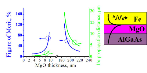
The Figure 1 shows 1/e propagation distance and MO Figure-of-Merit for plasmons in Fe/MgO/Al0.5Ga0.5As as a function of MgO thickness calculated using this method. The structure does not support the plasmons when MgO thickness is between 14 nm and 110 nm. Near "cutoff" thicknesses of 14 nm and 110 nm, the the plasmon's propagation distance increases from a few micrometers to 20 micromiters and importantly the MO FoM significantly increases from a few percents to above 100 %. It is very significant enhancement of the transverse MO effect. Remarkably, the MO effect is so large, that the magnetization dependent loss for the plasmons becomes comparable to normal optical loss.
Why there is a cutoff thickness for plasmons?
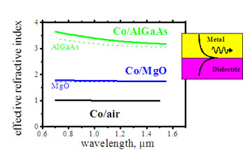
It is well-known that waveguide mode have cutoff in respect of thickness of a waveguide core layer. The reason for cutoff in case of the plasmons is different. In the following I will explain reason why there is a cutoff thickness for plasmons propagating in the structure with a double-layer dielectric. Firstly, I will recall one important property of plasmons in conventional structure with a single-layer dielectric. The Figure 2 shows the effective refractive index of the plasmons in the structure with a single-layer dielectric. Also, the refractive index of material of dielectric is shown in this figure. As can be seen, the value of the effective refractive index for plasmons is always very close to the value of refractive index of the dielectric. It is a very general property of the surface plasmons. Next, let us consider the plasmons in Fe/MgO/AlGaAs. It is obvious that in case when MgO thickness is very thick, the effective refractive index of plasmons is close to the refractive index of MgO. In the when MgO thickness is very thin, the effective refractive index of plasmons is close to the refractive index of AlGaAs. Since difference in refractive index of MgO and AlGaAs is large and the effective refractive index of plasmons can not be very different from the refractive index either of MgO or AlGaAs, in the case of intermediate MgO thickness the condition for plasmon propagation is not satisfied.
The following gives another explanation of the cutoff. Figure 3 shows the skin depth in the dielectric and the metal for plasmons in Fe/MgO/AlGaAs. When the MgO thickness approaches the cutoff, the skin depth in the metal practically does not change. In contrast, the skin depth in the dielectric sharply increase. That means that near cutoff there is a significant amount of optical field inside the dielectric and optical confinement by metal/dielectric interface becomes weak. When the thickness approaches the cutoff, the becomes weaker and weaker. Above the cutoff thickness there is no confinement anymore by metal/dielectric interface and plasmons can not propagate.
Why optical loss near cutoff is small?As can be seen from Fig.3, near cutoff the skin depth in dielectric is significantly larger than the skin depth in the metal. That means that the amount of optical field inside the dielectric is significantly larger than the amount of optical field inside the metal. Since the amount of optical field inside the metal is small, the plasmon's optical loss is small. It was known for the long time that the surface plasmons in the transition metal have huge loss. High optical loss has limited usage of surface plasmons in transition metals for practical applications. The structure with double-layer dielectric is a feasible method to reduce optical loss. Therefore, plasmons in the transition metals might have new applications.
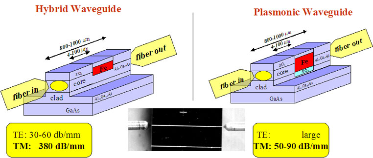
Why transverse MO effect is large?As can be seen from Fig.3, near cutoff the optical loss of optical plasmons sharply decreases near cutoff. It should be noticed that the value of cutoff thickness depends on optical constants of the metal and dielectrics. With reversal of metal's magnetization, due to transverse MO effect the effective optical constants of the metal slightly change. That leads to slight change of the value of cutoff thickness. In the case when MgO thickness is near cutoff thickness, from Fig.1 the slight MO change of value of cutoff thickness causes the large change of plasmon's loss. Therefore, in the case of the MgO thickness close to the "cutoff' thickness, a small MO change of the refractivity of the metal causes a significant MO change of plasmon's optical loss. That causes a substantial transverse MO effect. Experimental verification of low optical loss for surface plasmons in a structure with double-layer dielectricIn this experiment we fabricated two rather similar waveguides. One waveguide was hybrid waveguide and another waveguide was plasmonic waveguide. In both cases we used a rib AlGaAs waveguide (Al0.5Ga0.5As-clad, Al0.3Ga0.7As-core, SiO2-cover), which was transparent at operational light wavelength of 770 nm. The AlGaAs waveguide is used to deliver light to and out of the hybrid or plasmonic waveguide. The plasmonic or hybrid waveguide was fabricated in the middle of the AlGaAs waveguide. For this purpose inside the AlGaAs waveguide a pit was etched. In the case of the hybrid waveguide the etch was stopped near waveguide core and Fe was deposited inside the etch. In the case of the plasmon waveguide the pit was etched through the core layer inside of the cladding layer following SiO2 and Fe deposition. The waveguides with different length of the pit from 4 um to 100 um have been studied in order to estimate the optical loss. Even similar fabrication technology, the hybrid and plasmonic waveguides have very different properties. In the case of the hybrid waveguide, from the input to the output a waveguide mode propagates inside waveguide core slightly interacting with Fe. In the case of plasmonic waveguide the waveguide is fully etching and waveguiding mode is blocked by Fe. Therefore, there is one possible way the light from input can reach output. The input waveguide mode should excite a plasmon, the plasmon should propagate in Fe/SiO2/AlGaAs structure and the plasmon should excite an output waveguiding mode. Experimentally measured optical loss in hybrid and plasmonic waveguides was very different. In the case of hybrid waveguide the TE mode has relatively low optical loss comparing to TM mode. It is a very common feature of the hybrid waveguides. In contrast, in the case of the plasmonic waveguide I can see any TE polarized light passing through the structure, but TM mode showed surprisingly low optical loss. The loss even smaller than in the case of TM mode of hybrid waveguide. It is surprising, because in case of hybrid waveguide the waveguide core is fully open, but in the case of plasmonic waveguide the core is fully blocked. Since the plasmons can be only TM polarized, it is additional prove that light is passing by excitement of the plasmons.
|
I will try to answer your questions as soon as possible